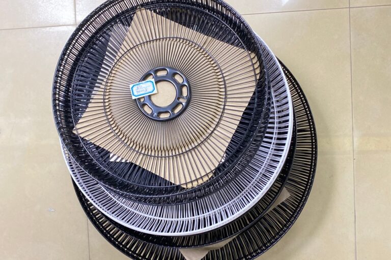
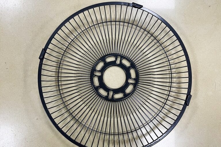
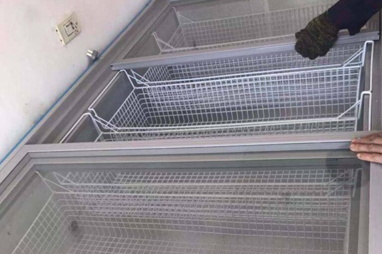
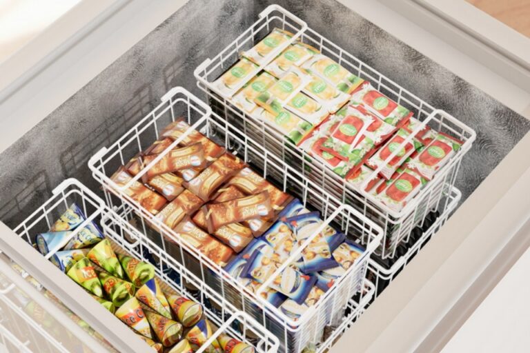
When a cooler or drink cabinet dies in the field, the end user only see “fridge broken”. But you and me know: often it’s a tiny PCB solder issue behind the pretty metal, glass, and wire shelves.
That’s why solid Solder Paste Inspection (SPI) is not “nice to have”. It’s basic survival for your SMT line, and for brands selling things like commercial display cabinet components or drink holder anti-tip wire rack systems together with smart controllers from partners like QIAO.
Why Solder Paste Inspection (SPI) Matters In PCB Assembly
Most process engineers will tell you a painful truth:
More than half of SMT defects come from the solder paste printing step.
If you only check after reflow, you already lost. You threw parts, time and line capacity into a board that was “doomed” at the printer.
Best practice 1: Put SPI right after printing, before placement.
- Treat SPI as the quality gate for printing.
- 100% boards go through SPI in mass production.
- Bad paste → board goes to reprint or rework, not into the pick-and-place queue.
Real-world scene:
You’re building control boards for a glass door merchandiser. If paste on a QFN power IC is low and nobody catch it, that board might fail inside a supermarket at 3 a.m. Compressor stops, drinks become warm, everybody angry. All started at the printer.

3D Solder Paste Inspection (SPI) vs 2D Inspection
Old lines still use 2D SPI or even only manual microscope. It works… until it doesn’t.
- 2D SPI checks shape and area from a camera.
- 3D SPI measures height and volume using structured light or laser.
Why 3D is now the standard for serious SMT lines:
- It detects paste volume, not just “it looks big enough”.
- It sees “pancake paste” – large area but very low height.
- It can better catch bridges and insufficient paste on fine-pitch pads.
In NPI builds or when you ramp a new board for a high-end refrigeration unit, use 3D SPI to tune print process until you get a stable “green” map. 2D can still help for simple, big pads, but don’t rely only on it for 0.5 mm BGA or tight QFN.
Solder Paste Volume And Height Tolerances In SPI
You can’t say “good” or “bad” paste print without numbers. Most EMS teams set target windows for volume and height relative to design.
A common starting point in many factories:
- Paste volume: 80–120% of design volume
- Paste height: around stencil thickness, with ±20% as working band
Then they tune it by product type.
Typical SPI Parameter Windows In PCB Assembly
| SPI Parameter | Typical Target Window (Start Point) | If Too Low | If Too High | Comment |
|---|---|---|---|---|
| Paste Volume (all pads) | 80–120% of design volume | Open joints, weak solder fillet | Bridging, solder balls, void risk | Adjust per component type |
| Paste Height | ~ stencil thickness ±20% | Not enough metal, “dry” joints | Slump, extra spread, tombstoning risk | Watch aging paste |
| X/Y Offset | < 25–50% of pad width | Fillet pulled off pad, partial opens | Same, plus risk on fine pitch bridges | Printer alignment / PCB fiducials |
| Area Coverage | > 80–90% of pad area | Corners bare copper, fillet too small | Usually tied to volume/height anyway | Check after stencil change |
| Bridges / Smearing | 0 allowed in mass production | No wetting, no bridge | Shorts, rework, NCMR, customer returns | Don’t negotiate here |
These numbers are not religion. Good process engineers use them as a starting recipe, then refine with real data: AOI results, x-ray for BGA, field returns.
Using SPI Data For Process Control In SMT Printing
If you only use SPI to say “Pass/Fail”, you’re wasting money. The real value is process control.
Daily routine on a modern line might look like this:
- Monitor SPC charts for paste volume and offset on key pads.
- When you see drift (for example, volume slowly goes down on one side), check:
- Squeegee pressure and speed
- Stencil cleaning frequency
- PCB support (bad tooling causes paste variation)
- Use a golden board and a “golden printer setup” as reference, so operators can bring the line back fast after changeover.
Example from a fridge controller job:
- You notice the paste volume on the relay pads trending up.
- SPI flags it as yellow, not yet red.
- Before you get real solder bridges, you stop, clean the stencil underside, adjust pressure a bit, and volume goes back to target.
- No downtime later, no field issue in a cold room full of frozen foods.

SPI Guidelines For Fine-Pitch BGA And QFN Components
Fine-pitch is where SPI really earn its money. For 0.5 mm BGA, QFN with big thermal pad, and small logic ICs, many factories use tighter windows:
- Volume: maybe 85–115% instead of 80–120%.
- Offset: closer to 25% or less of pad width.
Extra tips that show you know the craft:
- Use window-pane (segment) design on large thermal pads, then confirm paste distribution with 3D SPI.
- Increase stencil cleaning frequency for those zones; paste build-up there kills yield fast.
- In first article build, review SPI maps pad-by-pad for BGA sites before you trust the profile.
If you supply commercial display cabinet components or cold storage room components with smart controllers co-designed with QIAO, you want those BGAs solid. A single hidden void on a compressor driver can stop a whole line of merchandisers in a retail chain.
SPI Quality Standards And IPC-7527 Requirements
For serious customers (food retail, pharma cold rooms, supermarket chains), “looks good to me” is not enough. They expect you to reference industry standards like IPC-7527 for solder paste printing quality.
Best practice here:
- Align your SPI acceptance rules with IPC-7527 classes that match your market.
- Document what is acceptable, repairable, and reject for:
- pad coverage
- smearing
- slumping
- bridging
- Train operators with real photo examples, not only text. People remember pictures from real boards.
Turning SPI Data Into Real Factory Decisions
Let’s be real: nobody in production has time for pure academic stuff. SPI has to support takt time, yield and NPI ramp.
Here’s how mature teams use the data:
- Before mass run
- During NPI builds, they correlate SPI data with AOI and x-ray defects.
- If they see that 70–80% of certain solder defects come from low paste on a type of pad, they tighten the volume window there.
- During mass production
- They only stop the line when SPI crosses agreed limits, not on random noise.
- They log printer adjustments, stencil changes and cleaning in the same system as SPI results, so engineers can see full history.
This mindset works whether you assemble PCB for industrial freezers, vending machines, or lighting inside display cabinets. For a company like QIAO, which focuses on custom wire shelving manufacturing services and commercial display cabinet components, choosing EMS partners with strong SPI process is a smart risk control. Your metal parts keep the products standing, their PCBs keep them running.


